The End of Moore’s Law
I have been working on an upcoming post about megatrends and how they drive tech. I had included the end of Moore’s Law to illustrate how the end of a megatrend might also have a big influence on tech, but that section got away from me, becoming much larger than the sections on each individual current megatrend. So I decided to break it out into a separate post and publish it first. Here it is.
Moore’s Law, concerning what we put on silicon wafers, is over after a solid fifty year run that completely reshaped our world. But that end unleashes lots of new opportunities.
WHERE DID MOORE’S LAW COME FROM?
Moore, Gordon E., Cramming more components onto integrated circuits, Electronics, Vol 32, No. 8, April 19, 1965.
Electronics was a trade journal that published monthly, mostly, from 1930 to 1995. Gordon Moore’s four and a half page contribution in 1965 was perhaps its most influential article ever. That article not only articulated the beginnings, and it was the very beginnings, of a trend, but the existence of that articulation became a goal/law that has run the silicon based circuit industry (which is the basis of every digital device in our world) for fifty years. Moore was a Cal Tech PhD, cofounder in 1957 of Fairchild Semiconductor, and head of its research and development laboratory from 1959. Fairchild had been founded to make transistors from silicon at a time when they were usually made from much slower germanium.
One can find many files on the Web that claim to be copies of the original paper, but I have noticed that some of them have the graphs redrawn and that they are sometimes slightly different from the ones that I have always taken to be the originals. Below I reproduce two figures from the original that as far as I can tell have only been copied from an original paper version of the magazine, with no manual/human cleanup.
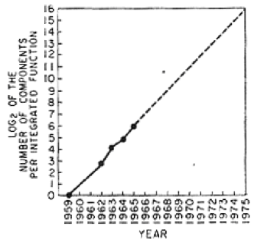
The first one that I reproduce here is the money shot for the origin of Moore’s Law. There was however an equally important earlier graph in the paper which was predictive of the future yield over time of functional circuits that could be made from silicon. It had less actual data than this one, and as we’ll see, that is really saying something.
This graph is about the number of components on an integrated circuit. An integrated circuit is made through a process that is like printing. Light is projected onto a thin wafer of silicon in a number of different patterns, while different gases fill the chamber in which it is held. The different gases cause different light activated chemical processes to happen on the surface of the wafer, sometimes depositing some types of material, and sometimes etching material away. With precise masks to pattern the light, and precise control over temperature and duration of exposures, a physical two dimensional electronic circuit can be printed. The circuit has transistors, resistors, and other components. Lots of them might be made on a single wafer at once, just as lots of letters are printed on a single page at one. The yield is how many of those circuits are functional–small alignment or timing errors in production can screw up some of the circuits in any given print. Then the silicon wafer is cut up into pieces, each containing one of the circuits and each is put inside its own plastic package with little “legs” sticking out as the connectors–if you have looked at a circuit board made in the last forty years you have seen it populated with lots of integrated circuits.
The number of components in a single integrated circuit is important. Since the circuit is printed it involves no manual labor, unlike earlier electronics where every single component had to be placed and attached by hand. Now a complex circuit which involves multiple integrated circuits only requires hand construction (later this too was largely automated), to connect up a much smaller number of components. And as long as one has a process which gets good yield, it is constant time to build a single integrated circuit, regardless of how many components are in it. That means less total integrated circuits that need to be connected by hand or machine. So, as Moore’s paper’s title references, cramming more components into a single integrated circuit is a really good idea.
The graph plots the logarithm base two of the number of components in an integrated circuit on the vertical axis against calendar years on the horizontal axis. Every notch upwards on the left doubles the number of components. So whilemeans
components,
means
components. That is a thousand fold increase from 1962 to 1972.
There are two important things to note here....MUCH MOREAnd from the high performance computing (supercomputing) mavens at Inside HPC, Feb. 24:
Beyond the Moore’s Law Cliff: The Next 1000X
In this video from the 2017 HPC Advisory Council Stanford Conference, Subhasish Mitra from Stanford presents: Beyond the Moore’s Law Cliff: The Next 1000X.
Professor Subhasish Mitra directs the Robust Systems Group in the Department of Electrical Engineering and the Department of Computer Science of Stanford University, where he is the Chambers Faculty Scholar of Engineering. Prior to joining Stanford, he was a Principal Engineer at Intel Corporation. He received Ph.D. in Electrical Engineering from Stanford University.
Prof. Mitra’s research interests include robust system design, VLSI design, CAD, validation and test, emerging nanotechnologies, and emerging neuroscience applications. His X-Compact technique for test compression has been key to cost-effective manufacturing and high-quality testing of a vast majority of electronic systems, including numerous Intel products. X-Compact and its derivatives have been implemented in widely-used commercial Electronic Design Automation tools. The QED and IFRA techniques, created jointly with his students, have shown outstanding results in overcoming critical bottlenecks in post-silicon validation and debug for several commercial hardware platforms, and have been characterized as “breakthrough” in a Research Highlight in the Communications of the ACM (CACM)....MORE, including the video.