From Works In Progress, May 14:
The strange path to global monopoly
The phones we carry around in our pockets have two million times more memory and are thousands of times faster than the room-sized computers that guided the Apollo mission to the Moon. This incredible shrinking act has been driven by our ability to make transistors smaller and smaller.
Each transistor is a microscopic switch that can alternate between a one and a zero, the basic language of all computing. Billions are packed onto tiny silicon chips called semiconductors. The more transistors that fit onto a chip, the more logic and memory circuits it holds, and the more it can do.
Advanced semiconductors are, arguably, the most important technology in the world. Over the last five years, they have even emerged as a geopolitical flashpoint between the US and China. But for all this rivalry, any country or company that hopes to manufacture semiconductors is dependent on a single firm: ASML. Dubbed ‘a relatively obscure Dutch company’ by the BBC in 2020, ASML makes the only machines in the world capable of stenciling the transistors onto chips with the precision necessary to fit billions on a 30-centimeter wafer.
These machines are roughly the size of double-decker buses. To ship one requires 40 freight containers, three cargo planes, and 20 trucks. They are the world’s most complex objects. Each contains over one hundred thousand components, all of which have to be perfectly calibrated for the machine to produce light consistently at the right wavelength.
While ASML is now the sole supplier of these machines, and will be for some time to come, it started out as a laggard in the chipmaking industry. Overtaking its competition required many things rarely associated with European companies: close collaboration with the American government, selling large stakes to foreign competitors, and a huge gamble on an unproven technology.
Let there be light
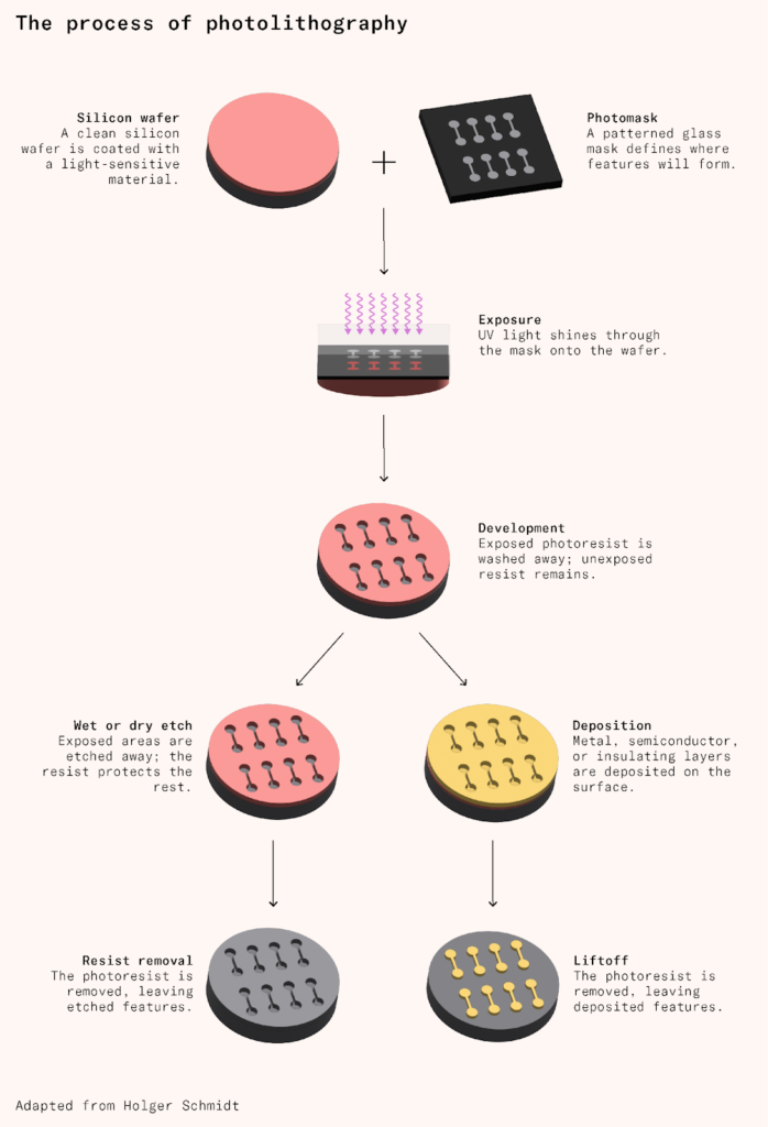
The key to ASML’s success is a technology called photolithography (sometimes just called lithography). The technique involves transferring a pattern onto a semiconductor wafer by exposing it to light. In the 1950s, the first chipmakers had tried to draw these patterns by hand, but anything that physically touches the wafer scratches it, dirties it, or warps the pattern. Scientists working independently for Bell Labs and the US military realized that they could use light to print identical patterns without making physical contact with the wafer.
To make chips, engineers start with a thin wafer of semiconductor material, usually silicon. This wafer is coated with a chemical called photoresist, which reacts when exposed to light. In photolithography, light is projected through a detailed pattern onto the photoresist-coated wafer, softening the exposed areas. The wafer is washed to remove any softened areas, revealing the silicon underneath. It is then moved to an etching machine that blasts it with charged chlorine or bromine gas, carving the desired pattern into the exposed silicon. These features are later filled with metal, such as tungsten and copper, to connect the transistor to power. These etched layers then combine into an intricate network of transistors.
Over time, the semiconductor manufacturing ecosystem has developed increasingly sophisticated etching using ever smaller wavelengths of light. Smaller wavelengths diffract less, allowing the light to travel in straighter lines and print sharper, tinier details without blurring. These allow for more precise pattern projections that, in turn, allow smaller and more densely packed transistors.
Early lithography relied on mercury vapor lamps that were similar to streetlights, while more modern machines rely on lasers created using argon and fluorine gases. By 2010, such lasers made it possible to create a 22-nanometer feature through multiple exposures using a 193-nanometer wavelength.
The most advanced version of this technology, extreme ultraviolet lithography, is used to make the very smallest chips. The smallest in 2025 were marketed as three nanometers, roughly 25,000 times thinner than a human hair.
To make them, a droplet of liquid tin is released into a chamber and hit with a single pulse of light, which melts and flattens it. As the droplet continues to fall, a second, more powerful pulse vaporizes the tin, creating an extremely hot plasma that emits light at the narrow wavelengths needed for extreme ultraviolet lithography. The light beam is then concentrated by reflecting it across a series of slightly concave mirrors so flawless that, if scaled to the size of Germany, their imperfections would be measured in millimeters. Engineers need to use mirrors, rather than the glass lenses used in standard lithography, as almost all solid materials absorb light at such short wavelengths.
The light eventually hits the mask, which contains the pattern to be printed on the chip. As the pattern on the mask is usually several times larger than what is wanted on the chip, the light is then reflected by a second system of mirrors....
....MUCH MORE