I see analysts, fund mangers and talking heads on the TV analyzing the chip supply line: ASML to TSM to NVDA, as if they were meme stocks, and it is just such a failure to understand what is happening—or at minimum to be humble in the face of their own ignorance of what is happening—that it borders on cosmic farce.
From IEEE Spectrum, March 28:
By Mark Liu and H.-S. Philip Wong
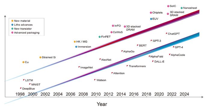
In 1997 the IBM Deep Blue supercomputer defeated world chess champion Garry Kasparov. It was a groundbreaking demonstration of supercomputer technology and a first glimpse into how high-performance computing might one day overtake human-level intelligence. In the 10 years that followed, we began to use artificial intelligence for many practical tasks, such as facial recognition, language translation, and recommending movies and merchandise.
Fast-forward another decade and a half and artificial intelligence has advanced to the point where it can “synthesize knowledge.” Generative AI, such as ChatGPT and Stable Diffusion, can compose poems, create artwork, diagnose disease, write summary reports and computer code, and even design integrated circuits that rival those made by humans.
Tremendous opportunities lie ahead for artificial intelligence to become a digital assistant to all human endeavors. ChatGPT is a good example of how AI has democratized the use of high-performance computing, providing benefits to every individual in society.
All those marvelous AI applications have been due to three factors: innovations in efficient machine-learning algorithms, the availability of massive amounts of data on which to train neural networks, and progress in energy-efficient computing through the advancement of semiconductor technology. This last contribution to the generative AI revolution has received less than its fair share of credit, despite its ubiquity.
Over the last three decades, the major milestones in AI were all enabled by the leading-edge semiconductor technology of the time and would have been impossible without it. Deep Blue was implemented with a mix of 0.6- and 0.35-micrometer-node chip-manufacturing technology. The deep neural network that won the ImageNet competition, kicking off the current era of machine learning, was implemented with 40-nanometer technology. AlphaGo conquered the game of Go using 28-nm technology, and the initial version of ChatGPT was trained on computers built with 5-nm technology. The most recent incarnation of ChatGPT is powered by servers using even more advanced 4-nm technology. Each layer of the computer systems involved, from software and algorithms down to the architecture, circuit design, and device technology, acts as a multiplier for the performance of AI. But it’s fair to say that the foundational transistor-device technology is what has enabled the advancement of the layers above.
If the AI revolution is to continue at its current pace, it’s going to need even more from the semiconductor industry. Within a decade, it will need a 1-trillion-transistor GPU—that is, a GPU with 10 times as many devices as is typical today.
Relentless Growth in AI Model Sizes
The computation and memory access required for AI training have increased by orders of magnitude in the past five years. Training GPT-3, for example, requires the equivalent of more than 5 billion billion operations per second of computation for an entire day (that’s 5,000 petaflops-days), and 3 trillion bytes (3 terabytes) of memory capacity.
Both the computing power and the memory access needed for new generative AI applications continue to grow rapidly. We now need to answer a pressing question: How can semiconductor technology keep pace?
From Integrated Devices to Integrated Chiplets
Since the invention of the integrated circuit, semiconductor technology has been about scaling down in feature size so that we can cram more transistors into a thumbnail-size chip. Today, integration has risen one level higher; we are going beyond 2D scaling into 3D system integration. We are now putting together many chips into a tightly integrated, massively interconnected system. This is a paradigm shift in semiconductor-technology integration.In the era of AI, the capability of a system is directly proportional to the number of transistors integrated into that system. One of the main limitations is that lithographic chipmaking tools have been designed to make ICs of no more than about 800 square millimeters, what’s called the reticle limit. But we can now extend the size of the integrated system beyond lithography’s reticle limit. By attaching several chips onto a larger interposer—a piece of silicon into which interconnects are built—we can integrate a system that contains a much larger number of devices than what is possible on a single chip. For example, TSMC’s chip-on-wafer-on-substrate (CoWoS) technology can accommodate up to six reticle fields’ worth of compute chips, along with a dozen high-bandwidth-memory (HBM) chips.
HBMs are an example of the other key semiconductor technology that is increasingly important for AI: the ability to integrate systems by stacking chips atop one another, what we at TSMC call system-on-integrated-chips (SoIC). An HBM consists of a stack of vertically interconnected chips of DRAM atop a control logic IC. It uses vertical interconnects called through-silicon-vias (TSVs) to get signals through each chip and solder bumps to form the connections between the memory chips. Today, high-performance GPUs use HBMextensively.
Going forward....
....MUCH MORE