First up, from Bloomberg, November 25:
Alphabet AI Chips, Gemini Model Position It to Rival Nvidia
A rally in Alphabet Inc. shares is poised to shake up the ranking of the world’s most valuable companies, amid signs the search giant is making headway in efforts to rival Nvidia Corp.’s bestselling AI accelerator.
That’s prompting investors to reassess the technology landscape and the potential changes in stock market leadership, as rave reviews for Alphabet’s new Gemini artificial intelligence model and demand for AI chips pushes its shares higher.
Shares in the Mountain View, California-based firm rallied 2% to hit a $3.9 trillion market value. Its 37% rally since mid-October has added about $1 trillion in value over that time. Gains this year have left the Google parent about $300 billion away from Nvidia’s $4.2 trillion market cap.
Meta Platforms Inc. is in discussions to use Google chips — known as tensor processing units, or TPUs — in data centers in 2027, The Information reported, citing an unidentified person familiar with the talks. Meta also may rent chips from Google’s cloud division next year, the news outlet said.
“Nvidia is expected to have phenomenal growth and now it will be very natural to see a market that is much more wary of competition,” said Alexandra Morris, an investment director at Skagen AS. “The narrative that Nvidia is the only one that will provide chips to this buildup of data centers — that narrative has changed.”
An agreement with Meta would help establish TPUs as an alternative to Nvidia’s chips, the gold standard for big tech firms and startups from Meta to OpenAI that need computing power to develop and run AI models.
Read More: Nvidia Shares Drop on Report of Google Challenge in AI Chips
Nvidia slipped 5.1%, while shares in smaller-rival Advanced Micro Devices Inc., which also makes AI chips, fell 7.8%.
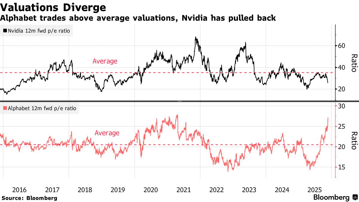
Nvidia’s valuations have pulled back, trading at 26 times forward earnings, well below its average over the past decade of 35 times. Alphabet’s has shot up to trade at 27 times forward earnings compared to an average of 20 times.
While a possible deal with Meta — one of the biggest spenders globally on data centers and AI development — draws attention to the potential for long-term challenges to Nvidia’s dominant market position, much depends on whether the tensor chips can demonstrate the power efficiency and computing muscle necessary to become a viable option in the long run.
This frenzy is causing Alphabet stock’s 14-day relative strength index to about 75, over the level of 70 that signals to some technical analysts that a stock is overbought...
....MORE
While we've been tracking the GOOG's TPU progress for a decade, this morning Zerohedge found a dandy little write-up on the chips that we'll go with rather than use back-links.
From UncoverAlpha, November 24:
The chip made for the AI inference era – the Google TPU
Hey everyone,
As I find the topic of Google TPUs extremely important, I am publishing a comprehensive deep dive, not just a technical overview, but also strategic and financial coverage of the Google TPU.
Topics covered:
The history of the TPU and why it all even started?
The difference between a TPU and a GPU?
Performance numbers TPU vs GPU?
Where are the problems for the wider adoption of TPUs
Google’s TPU is the biggest competitive advantage of its cloud business for the next 10 years
How many TPUs does Google produce today, and how big can that get?
Gemini 3 and the aftermath of Gemini 3 on the whole chip industry
Let’s dive into it.
The history of the TPU and why it all even started?
The story of the Google Tensor Processing Unit (TPU) begins not with a breakthrough in chip manufacturing, but with a realization about math and logistics. Around 2013, Google’s leadership—specifically Jeff Dean, Jonathan Ross (the CEO of Groq), and the Google Brain team—ran a projection that alarmed them. They calculated that if every Android user utilized Google’s new voice search feature for just three minutes a day, the company would need to double its global data center capacity just to handle the compute load.
At the time, Google was relying on standard CPUs and GPUs for these tasks. While powerful, these general-purpose chips were inefficient for the specific heavy lifting required by Deep Learning: massive matrix multiplications. Scaling up with existing hardware would have been a financial and logistical nightmare.
This sparked a new project. Google decided to do something rare for a software company: build its own custom silicon. The goal was to create an ASIC (Application-Specific Integrated Circuit) designed for one job only: running TensorFlow neural networks.
Key Historical Milestones:
2013-2014: The project moved really fast as Google both hired a very capable team and, to be honest, had some luck in their first steps. The team went from design concept to deploying silicon in data centers in just 15 months—a very short cycle for hardware engineering.
2015: Before the world knew they existed, TPUs were already powering Google’s most popular products. They were silently accelerating Google Maps navigation, Google Photos, and Google Translate.
2016: Google officially unveiled the TPU at Google I/O 2016.
This urgency to solve the “data center doubling” problem is why the TPU exists. It wasn’t built to sell to gamers or render video; it was built to save Google from its own AI success. With that in mind, Google has been thinking about the »costly« AI inference problems for over a decade now. This is also one of the main reasons why the TPU is so good today compared to other ASIC projects.
The difference between a TPU and a GPU?
To understand the difference, it helps to look at what each chip was originally built to do. A GPU is a “general-purpose” parallel processor, while a TPU is a “domain-specific” architecture.
The GPUs were designed for graphics. They excel at parallel processing (doing many things at once), which is great for AI. However, because they are designed to handle everything from video game textures to scientific simulations, they carry “architectural baggage.” They spend significant energy and chip area on complex tasks like caching, branch prediction, and managing independent threads.
A TPU, on the other hand, strips away all that baggage. It has no hardware for rasterization or texture mapping. Instead, it uses a unique architecture called a Systolic Array.
The “Systolic Array” is the key differentiator. In a standard CPU or GPU, the chip moves data back and forth between the memory and the computing units for every calculation. This constant shuffling creates a bottleneck (the Von Neumann bottleneck).
In a TPU’s systolic array, data flows through the chip like blood through a heart (hence “systolic”).
It loads data (weights) once.
It passes inputs through a massive grid of multipliers.
The data is passed directly to the next unit in the array without writing back to memory.
What this means, in essence, is that a TPU, because of its systolic array, drastically reduces the number of memory reads and writes required from HBM. As a result, the TPU can spend its cycles computing rather than waiting for data.
Google’s new TPU design, also called Ironwood also addressed some of the key areas where a TPU was lacking:
They enhanced the SparseCore for efficiently handling large embeddings (good for recommendation systems and LLMs)
It increased HBM capacity and bandwidth (up to 192 GB per chip). For a better understanding, Nvidia’s Blackwell B200 has 192GB per chip, while Blackwell Ultra, also known as the B300, has 288 GB per chip.
Improved the Inter-Chip Interconnect (ICI) for linking thousands of chips into massive clusters, also called TPU Pods (needed for AI training as well as some time test compute inference workloads). When it comes to ICI, it is important to note that it is very performant with a Peak Bandwidth of 1.2 TB/s vs Blackwell NVLink 5 at 1.8 TB/s. But Google’s ICI, together with its specialized compiler and software stack, still delivers superior performance on some specific AI tasks.
The key thing to understand is that because the TPU doesn’t need to decode complex instructions or constantly access memory, it can deliver significantly higher Operations Per Joule.
For scale-out, Google uses Optical Circuit Switch (OCS) and its 3D torus network, which compete with Nvidia’s InfiniBand and Spectrum-X Ethernet. The main difference is that OCS is extremely cost-effective and power-efficient as it eliminates electrical switches and O-E-O conversions, but because of this, it is not as flexible as the other two. So again, the Google stack is extremely specialized for the task at hand and doesn’t offer the flexibility that GPUs do.
Performance numbers TPU vs GPU?
As we defined the differences, let’s look at real numbers showing how the TPU performs compared to the GPU. Since Google isn’t revealing these numbers, it is really hard to get details on performance. I studied many articles and alternative data sources, including interviews with industry insiders, and here are some of the key takeaways.
The first important thing is that there is very limited information on Google’s newest TPUv7 (Ironwood), as Google introduced it in April 2025 and is just now starting to become available to external clients (internally, it is said that Google has already been using Ironwood since April, possibly even for Gemini 3.0.). And why is this important if we, for example, compare TPUv7 with an older but still widely used version of TPUv5p based on Semianalysis data:
TPUv7 produces 4,614 TFLOPS(BF16) vs 459 TFLOPS for TPUv5p
TPUv7 has 192GB of memory capacity vs TPUv5p 96GB
TPUv7 memory Bandwidth is 7,370 GB/s vs 2,765 for v5p
We can see that the performance leaps between v5 and v7 are very significant. To put that in context, most of the comments that we will look at are more focused on TPUv6 or TPUv5 than v7.
Based on analyzing a ton of interviews with Former Google employees, customers, and competitors (people from AMD, NVDA & others), the summary of the results is as follows.....
....MUCH MORE
Nvidia is getting whacked for $10.62 (-5.82%) to $171.93 while GOOG is up another1.99% (+$6.33)
Related, November 24 - Trouble In Altman's World: "I’m Not Going Back To ChatGPT After Using Google’s Gemini 3: Salesforce CEO Marc Benioff"