This gentleman, William Huo, seems a bit too cocksure that China will leave the West in the dust but he points out some interesting recent advances.
First up, the tweet pinned at the top of his X feed:
I’ve come to see my tweets not as commentary but as a running chronicle of history. Each one marks a watershed moment in China’s push to reclaim its rightful place in the global order.https://t.co/gU1oNuInCx
— William Huo (@wmhuo168) June 14, 2025
And the beginning of his thread:
On July 19, 2025, China killed the silicon wafer. And with it, ASML’s monopoly, TSMC’s moat, and every American chip sanction. You just didn’t hear the explosion. Time to break it down. (1/21)https://t.co/v2fFYwXEWW
— William Huo (@wmhuo168) July 20, 2025
Because we (Climateer Investing and yours truly) are not on X (or any of the competing platforms) we are dependent on others to call upon Threadreader to unroll anything over one tweet. Here goes:
On July 19, 2025, China killed the silicon wafer. And with it, ASML’s monopoly, TSMC’s moat, and every American chip sanction. You just didn’t hear the explosion. Time to break it down. (1/21)
Part I: The Atomic Truth
Most people think the chip war is about geopolitics. It’s not. It’s about atomic ratios. And China just mastered a law of nature the West still struggles to pronounce: stoichiometry.(2/21)
Stoichiometry is the a priori rulebook for matter. Not a lab trick. Not engineering. It’s the logic atoms obey when forming compounds. You get the ratios right or the structure collapses. Period. (3/21)
Silicon is forgiving. You can tweak and etch and polish. Add more doping. Fix things post-growth. That’s why the entire Western chip industry is addicted to photolithography and brute-force scaling. (4/21)
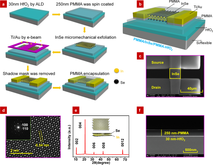
Indium selenide (InSe) is not forgiving. It’s a 2D compound. One atom thick. One indium per selenium. Anything less than perfect stoichiometry? You get garbage. Defects. No chip. No circuit. (5/21)
That’s what makes China’s breakthrough historic. Their scientists didn’t invent InSe. They cracked how to grow it perfectly. At scale. With atomic self-correction. No ASML needed. No permission slip.(6/21)
Their method vaporizes indium, condenses it into a liquid layer, and grows InSe by balancing the atomic ratio in real time. The process self-regulates the stoichiometry. That’s the key.(7/21)
They didn’t stop at flakes. They built 5 cm wafers. They etched transistor arrays. They proved it works on a chip, not just under an electron microscope. It’s fabrication-grade.(8/21)This isn’t a lab paper. It’s the exit wound from the silicon era. The stoichiometric bottleneck is gone. The rest is just assembly.(9/21)Part II: After Silicon
InSe outperforms silicon in every category that matters:
• 5–10x higher electron mobility
• Atomic thickness
• Tunable bandgap
• Lower power leakage
• Faster switching (10/21) ....
....MUCH MORE
Though not directly related, this July 17 article at IEEE Spectrum may also be of interest:
2D Transistors Could Come Sooner Than Expected
CDimension thinks it can cut the 10-year timeline in half