First up, from The Next Platform, March 28:
How To Build A Better “Blackwell” GPU Than Nvidia Did
While a lot of people focus on the floating point and integer processing architectures of various kinds of compute engines, we are spending more and more of our time looking at memory hierarchies and interconnect hierarchies. And that is because compute is easy, and data movement and memory are getting harder and harder.
To put some simple numbers on this: Over the past two decades, CPU and then GPU compute capacity has increased by a factor of 90,000X, but DRAM memory bandwidth has only increased by 30X and interconnect bandwidth has also only increased by 30X. We have gotten better in some ways in recent years, but we think that the compute-memory balance is still far out if whack, and it means we are overspending on under-memoried compute engines for a lot of AI and HPC workloads.
It is with this in mind that we consider the architectural innovations at the physical layer, or PHY, in networks that have been created by Eliyan and that are being cast in a different and very useful light this week at the MemCon 2024 conference. Co-founder and chief executive officer Ramin Farjadrad took some time to show us how the NuLink PHY and its use cases have evolved over time, and how they can be used to build better, cheaper, and more powerful compute engines than can be done with current packaging techniques based on silicon interposers.
A PHY is a physical network transport device that links a switch chip, a network inferface, or any number of other kinds of interfaces on or within a compute engine to the physical media – copper wires, optical fibers, radio signals – that in turn connects them to each other or to a network.
A silicon interposer is the special circuitry bridge that is used to connect HBM stacked DRAM memory to compute engines such as GPUs and custom ASICs that are commonly used in bandwidth sensitive applications in the HPC and AI arenas. Sometimes HBM is used regular CPUs that are also in need of memory with high bandwidth.
Eliyan was founded in 2021 in San Jose and has grown to 60 people. The company has just taken down its second round of funding for $60 million, with memory maker Samsung and Tiger Global Capital leading the Series B round. Eliyan raised $40 million in its Series A round in November 2022, led by Tracker Capital Management with contributions from Celesta Capital, Intel, Marvell, and memory maker Micron Technology.
Farjadrad cut his teeth as a design engineer at Sun Microsystems and LSI Logic during the Dot Com Boom, was a switch ASIC chief engineer and co-founder at Velio Communications (now part of LSI Logic), and was a co-founder and chief technology officer at Aquantia, which made Ethernet PHYs for the car market. In September 2019, Marvell acquired Aquantia and put Farjadrad in charge of networking and automotive PHYs. Marvell has become one of the largest makers of PHYs, and competes against the likes of Broadcom, Alphawave Semi, Nvidia, Intel, Synopsis, Cadence, and now Eliyan in designing these key components of systems.
Eliyan’s other co-founders include Syrus Ziai, who is head of engineering and operations and who has been vice president of engineering at Ikanos, Qualcomm. PsiQuantum, and Nuvia over the years, and Patrick Soheili, who is head of business and corporate development and who was previously in charge of product management and head of AI strategy for eSilicon. This company is famous for creating the ASICs inside of Apple’s iPod music player and for developing 2.5D ASIC packaging and HBM memory controllers. And of course, eSilicon was acquired by Inphi in late 2019 for $213 million, broadening its PHY capabilities, and in April 2021 Marvell completed the circle by acquiring Inphi in October 2020 for $10 billion.
There is money is PHYs as well as in I/O SerDes and retimers. A SerDes, like those used in switch ASICs to convert parallel data coming out of a device to serial data pumped down a wire or a fiber or over the air, is a special kind of PHY, and to a certain way of thinking, so is a retimer, which will be increasingly used as bandwidth goes up and the length of a copper wire that can push a clean signal consequently goes down.
Fee PHY Faux Big Sum, we say. With that, let’s talk about 2.5D packaging for a minute.
Get Out Your 2.5D Glasses
As Moore’s Law increases in transistor density have slowed and the cost of transistors have come up with each successive process technology rather than going down, we have all been made aware of the reticle limit of modern chip etching processes. With plain vanilla extreme ultraviolet (EUV) water immersion lithography, the maximum size you can etch transistors onto a silicon wafer is 26 millimeters by 33 millimeters.
But many of us are perhaps not aware that is also a limit to the size of the silicon interposer that allows chiplets to be linked to each other on top of the organic substrate that is like a motherboard underneath each compute engine socket and its affiliated HBM memory. The size of that silicon interposer depends on the technology that is used to create the middleboard. (Well, that is what it is.) The interposers are made using the same lithography processes as chips are, but instead of having a reticle limit of 858 mm2 as the chip has, the interposer can be 2,500 mm2 today using some techniques, and closer to 1,900 mm2 using others; there are plans to push that up to 3,300 mm2 according to Farjadrad. Organic substrate sockets do not have such areal limitations. And this is important when you talk about 2.5D packaging of chiplets.
Farjadrad walked us through the feeds, speeds, and limitations of the different 2.5D approaches that Eliyan’s NuLink PHY competes with.
Here is how Taiwan Semiconductor Manufacturing Co does 2.5D with its Chip on Wafer on Silicon (CoWoS) process, which is used to create Nvidia and AMD GPUs and their HBM stacks, among other things:....
....MUCH MORE
Or, for the hobbyist, from Hackaday, October 27, 2023:
Build An Easy Replica Of HAL 9000
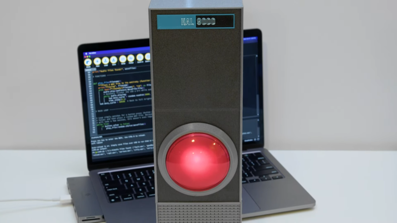
Adafruit’s PropMaker Feather is a microcontroller board designed specifically for building props with electronic features. Thus, what better way to show it off than by building a nifty replica of the most menacing AI ever to roam this solar system? That’s right, it’s the Adafruit HAL9000 build!
Following the 80/20 rule, this version is intended to be reasonably authentic while remaining affordable and easy to build. It’s built around Adafruit’s existing Massive Red Arcade Button, which looks like a decent simulacra of HAL9000’s foreboding, perceptive lens. It’s placed in a case assembled from laser-cut acrylic, with a neat inkjet-printed label on top. Where previously, sound effects were courtesy of an Arduino Uno with a Wave Shield, this version uses the PropMaker Feather, based on the RP2040, instead. It’s actually possible to assemble with zero soldering thanks to quick-connect wires and screw terminals on the PropMaker Feather.
Fundamentally, if you’re building a simple prop that needs audio or LEDs, the PropMaker Feather could be a useful tool for the job. Alternatively, consider building a HAL replica with more capability, like controlling your home. Just don’t give it too much responsibility—we all know how that ends. Video after the break....
....MORE
Among the comments:
That is great, I’ll be so sad when he murders you.